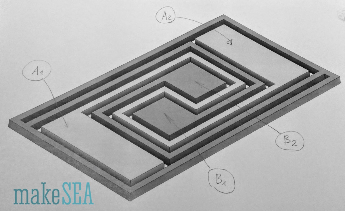
Now I know, how the conductive PLA from Proto Pasta can transport current. Apart from powering devices which consume more than 20-50 mA, this material could be very useful for low-power circuits. Consuming a lot of energy isn't a good idea anyway, because there are more and more electronic devices on earth, which in total waste a lot of energy. So I'm curious to see, if it's possible to design a simple PCB and check, if different wires are well isolated, if there is another material printed between.
For this test I've designd two conductors, which are running in parallel for a long distance. If the material in-between is not well isolating, the leaking current is easily measurable (the shape of the isolator is like a very short conductor with a large cross-section area).
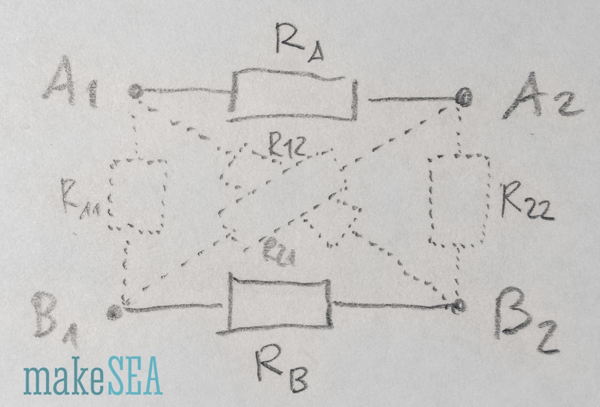
The electrical circuit scheme looks like this:
 |  |
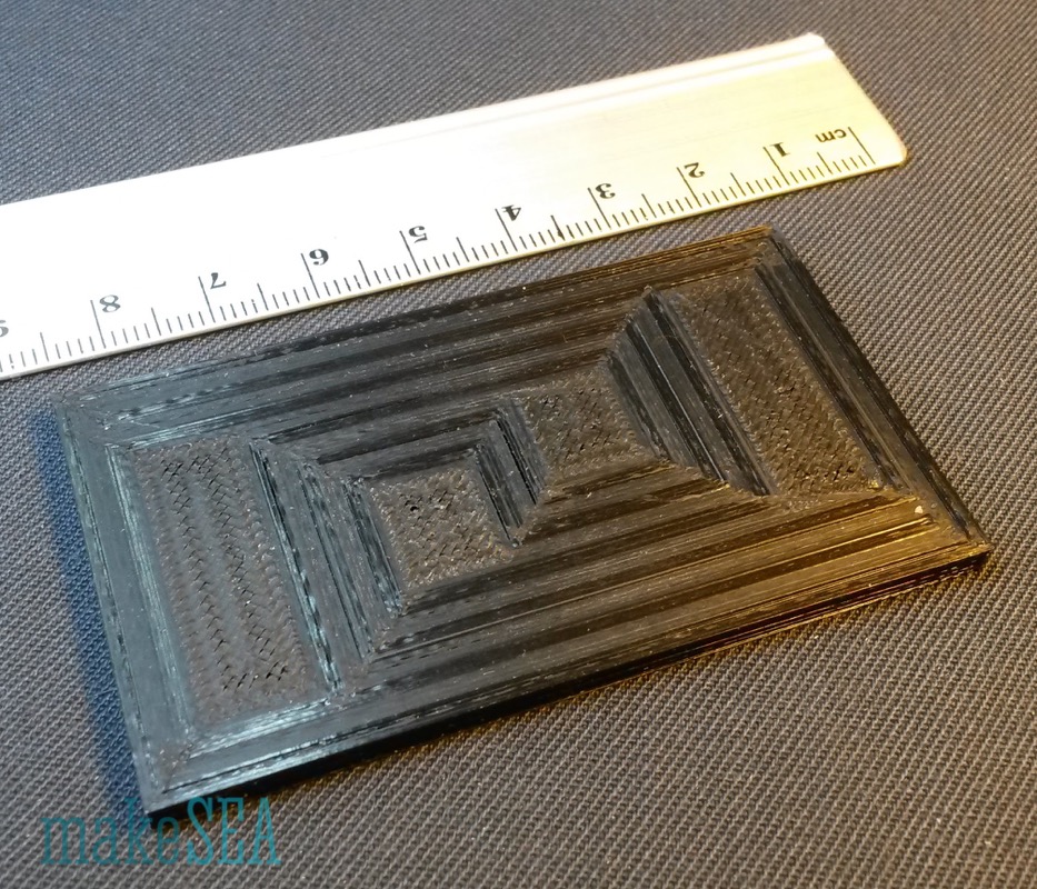
Because I only have regular PLA in black (printing mistakes difficult to see by eye when combined with the conductive black PLA), I started my experiments with blue ABS (230°C). What a mess, catastrophe! I really had big toubles to get a clean print. Initially adhesion to the build-plate was a problem and it heavily warped. After replacing the capton tape, increasing the temperatures (lower cooling), it did stick well, but the conductive PLA was clogging in the nozzle. Finally it worked with a build-plate temperature of 120°C, enough lubrication, and the fan blowing at the print-head (and not too much at the build-plate). But visually I could already see thet the blue ABS had black cords from the PLA (even though I had activated purge-walls, and tried with both slicers Makerbot and Simplify3D) - the resistance from all 4 contact points was approximately the same ... big FAIL!
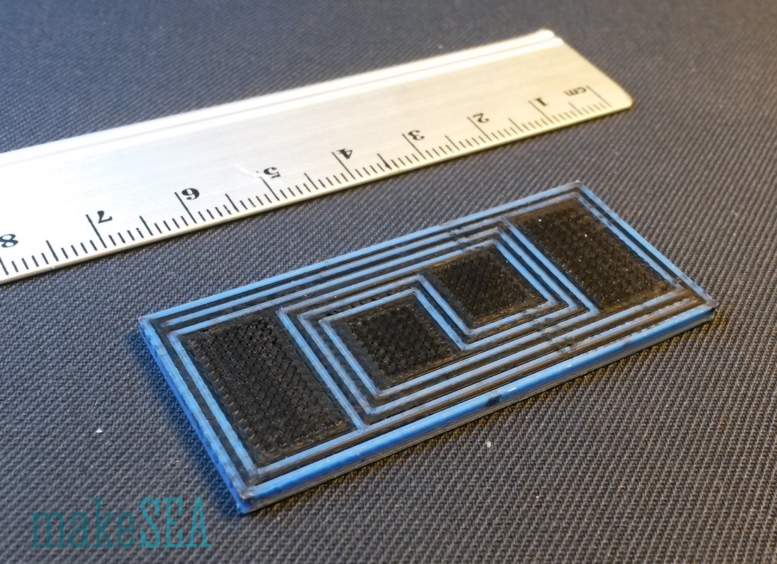 |  | 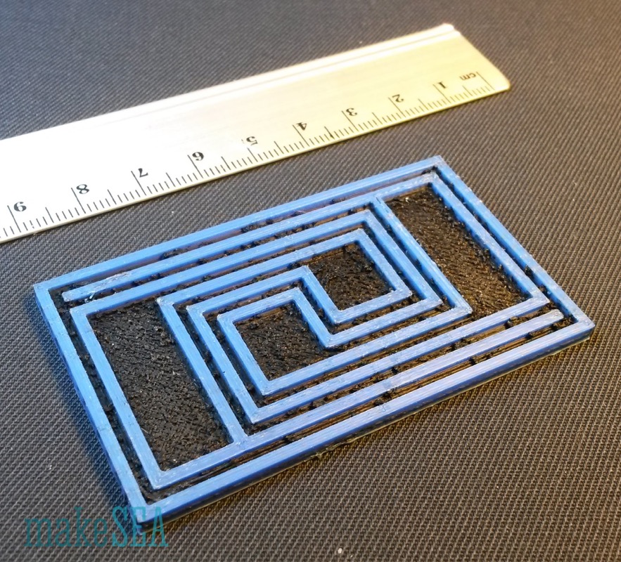 |
| Experiment A - ABS, 0.8 mm isolator | Experiment B - ABS, 1.6 mm isolator | Experiment C - ABS, PLA clogged nozzle |
Probably the higher ABS-temperature was causing the conductive PLA to melt, and even though the idle nozzle was clean, the ABS-nozzle was moving over PLA and picked up and distributed some of the printed conductive material. So I decided to try with my red PETG which can be printed with the same temperature as PLA at 205°C. And the build-plate only needs 80°C for great adhesion during print, and simple removing from capton after print (using water-alcohol mix) ... the versed reader will notice, that I'm a big fan of PETG ;-)
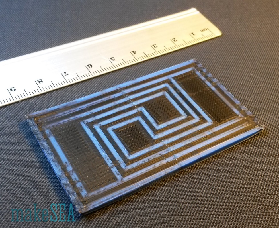
Unfortunately the initial experiments with PETG were not much better (Experiment D), but then I had the idea to rotate the object on the build-platform (smaller dimension oriented in x-direction). As a result the idle extrusion nozzle was moving much less over the printed area. Experiment E was the first successful print. Well recognizable the much cleaner print.
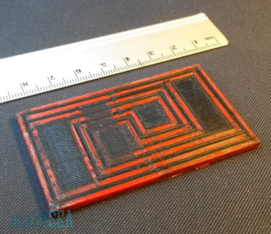 | 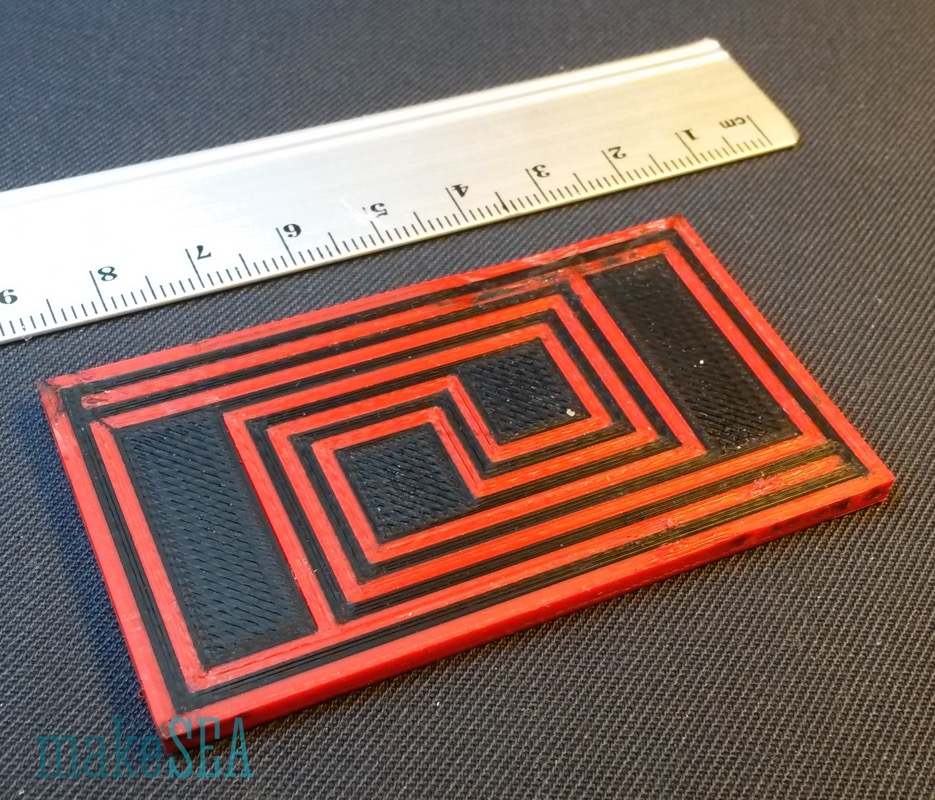 |  |
| Experiment D - PETG, 1.6 mm isolator | Experiment E - PETG, 1.6 mm, rotated print | Experiments all failed with PETG, 0.8 mm |
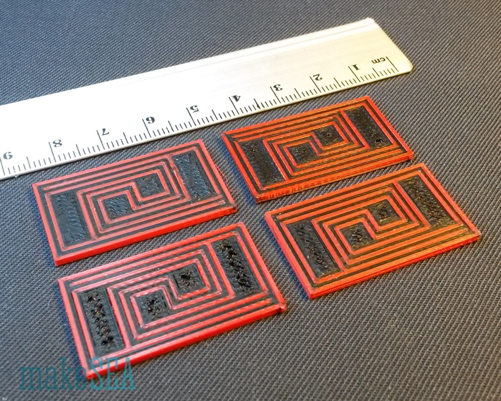
Encouraged by this success, I scaled the design down to 50% (with wires and isolators 0.8 mm wide - i.e. exactly 2 shells and no infill needed). I was set back to reality. None of these experiments suceeded. I tried with both slicers, reduced material flow and infill, but it never worked. Then I had a closer look at the nozzles (I should have taken a picture). Even thogh the printed result looked clean, the nozzle which was extruding the isolating red PETG had a messy black skirt - black conductive PLA, which it had picked up during some travel moves. Maybe the nozzle height was not well calibrated? For this reason I unloaded the materials, and reloded it right and left swapped. Same result, this time the other nozzle (again the nozzle extruding red PETG) had a black skirt. The other nozzle with the conductive PLA was always clean (resp. there was no red PETG skirt visible).
Final experiments: use regular PLA as isolator (unfortunately black and not as good visible on the pictures):
 | 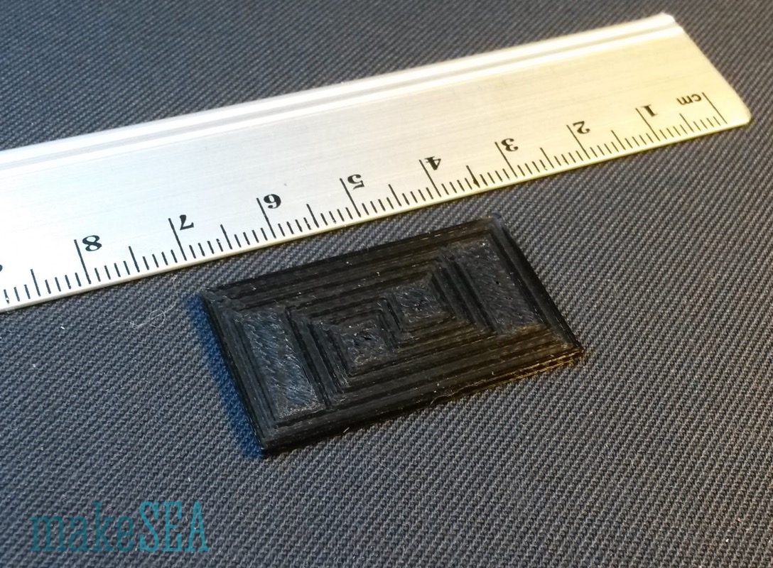 |
| Experiment F - PLA isolator 1.6 mm | Experiment G - PLA isolator 0.8 mm |
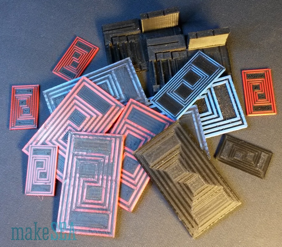
Hurray! :-) both succeded. No black skirt at the nozzles after printing - all nozzles were clean, and also the prints. Here is a table with all the detailed measurements.
| Experiment | A | B | C | D | E | F | G |
| A1 - A2 [kOhm] | 9.5 | 4.8 | 5.1 | 4.1 | 8.1 | 6.9 | 10.1 |
| B1 - B2 [kOhm] | 9.5 | 5.7 | 3.1 | 5.0 | 11.5 | 10.0 | 16.5 |
| A1 - B1 [kOhm] | 8.5 | 5.3 | 3.3 | 4.5 | 4'800.0 | > 20'000.0 | 330.0 |
| A1 - B2 [kOhm] | 4.2 | 6.3 | 3.7 | 3.4 | 4'800.0 | > 20'000.0 | 325.0 |
| A2 - B1 [kOhm] | 12.5 | 4.8 | 3.5 | 5.3 | 4'800.0 | > 20'000.0 | 320.0 |
| A2 - B2 [kOhm] | 9.1 | 6.5 | 5.1 | 4.9 | 4'800.0 | > 20'000.0 | 315.0 |
| Isolator Material | ABS blue | ABS blue | ABS blue | PETG red | PETG red | PLA black | PLA black |
| Isolator Temperature [°C] | 230 | 230 | 230 | 205 | 205 | 205 | 205 |
| Print Orientation | horizontal | horizontal | horizontal | horizontal | vertical | vertical | vertical |
| Isolation Width [mm] | 0.8 | 1.6 | 1.6 | 1.6 | 1.6 | 1.6 | 0.8 |
| Wire Section Area [mm^2] | 3.2 | 3.2 | 3.2 | 3.2 | 3.2 | 0.8 | |
| Wire Length A [mm] | 140 | 140 | 140 | 140 | 140 | 70 | |
| Wire Length B [mm] | 237 | 237 | 237 | 237 | 237 | 118.5 | |
| Resistivity A [kOhm*mm] | 0.11 | 0.12 | 0.09 | 0.19 | 0.16 | 0.12 | |
| Resistivity B [lOhm*mm] | 0.08 | 0.04 | 0.07 | 0.16 | 0.14 | 0.11 | |
| Result / Comment | fail | fail | fail | fail | ok | success | ok, but ... |
While the result E) with PETG is good, the result with PLA as isolator F) is excellent. My instrument can't measure more than 20 MOhm. Also G) is satisfactory, considering the extreme test-case. If shorter wires are used, and if it's not a circuit with very sensitive measurements, 0.8 mm thin isolators are well usable in a design.
These are all my experiments to get familiar with with conductive PLA. It wasn't trivial to get this material under control: if the result looks visually OK, it doesn't yet mean that it's also electrically OK.
Conclusion:
Infill and clean extrusion is key. Basically you would want to have 100% because the inferior conductivity of the conductive PLA. But if it overextrudes, there will be a big mess, and the circuilt fails. The possibilities and combinations of slicing options are huge. After all these experiments I guess ideally the isolator was printed with a single shell, and medium-low infill. The conductor probably as well with little infill, but with a big number of shells (filling the inside along the conducting direction). Avoid travel moves over "foreign" areas for both nozzles. Optimized travel moves of the idle nozzle can only be achieved, if the circuit design is not wider than the distance between the two extruders. Simplify3D theoretically is able to be tuned individually different for both extruders, but I had problems with the purge-walls. They did fall apart during printing. Makerbot has great working purge-walls with "spew-pots", but it has much less tuning options.
Conductive PLA sourced from:

3D-Model:
- STL ConductorA, ConductorB, Isolator
- STEP
- F3D